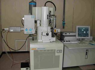
Field emission scanning electron microscopy
![]() FESEM:
FESEM:
Resolution : 1.0 nm (15kV), 2.2 nm (1kV)
Accelerating Voltage : 0.5 – 30kV
Magnification : 25 – 650,000
![]() BEM -
BEM -
![]() EDS
-
energy dispersive spectroscopy
EDS
-
energy dispersive spectroscopy
![]() CL
- cathodoluminescence
CL
- cathodoluminescence
Scanning range : 160 ~ 1200 nm
Spectral resolution : 0.1 nm
![]()
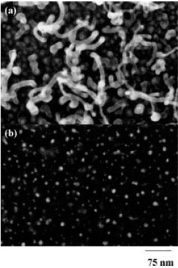
Top view FESEM images of carbon nanotubes grown for only 40 s on Fe-coated si substrate with a Fe-layer thickness of 7 nm taken in a) secondary electron imaging (SEI) mode b) backscatter electron imaging (BEI) mode.
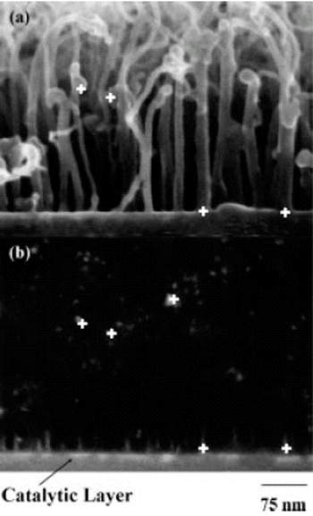
Corss-sectional FESEM images of CNT samples indicate the identical pairs of points of the sample in the SEI and BEI modes.
L. C. Chen, C. Y. Wen, C. H. Liang, W. K. Hong, K. J. Chen, H. C. Cheng, C. S. Shen, C. T. Wu and K. H. Chen, Advanced Functional Materials 12, 687 (2002).
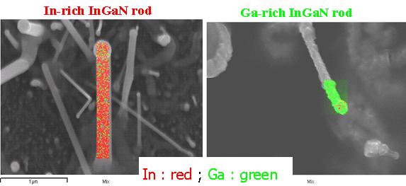
The EDS mapping
Hexagonal-to-cubic phase transformation in GaN nanowires by Ga+ implantation
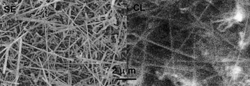
SE and CL (excited at 3.3 eV) images at 4 K showing large of the nanowires are in cubic phase.
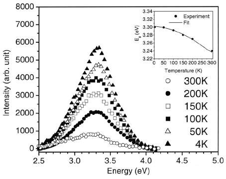
Temperature dependent CL spectra for the postannealed nanowires irradiated with an optimum fluence of 5 × 10⁻² cm-2 showing the presence of cubic GaN. Inset shows the temperature dependence of the band-to-band transition peak energies.
S. Dhara, A. Datta, C. T. Wu, Z. H. Lan, K. H. Chen, and Y. L. Wang, C. W. Hsu, C. H. Shen, and L. C. Chen, and C. C. Chen, Appl. Phys. Lett. 84, 5473 (2004).
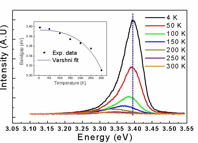
The CL spectra of temperature dependence, sample : ZnO Single nanorod with 100 nm diameter

CL spectra of single GaN nanorod indicate a slight blue shift with the diameter of nanorod increasing.
Acceleration voltage resolved CL spectra of InGaN film
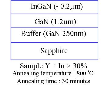

The 3, 5, 8, and 15 kV electron voltages roughly correspond to the penetration depths of 88, 210, 450, and 1300 nm.
S. W. Feng, T. Y. Tang, Y. C. Lu, S. J. Liu, E. C. Lin, C. C. Yang, K. J. Ma, C. H. Shen, L. C. Chen, K. H. Kim, J. Y. Lin, H. X. Jiang, J. Appl. Phys. 95, 5388 (2004).