![]()
![]() .
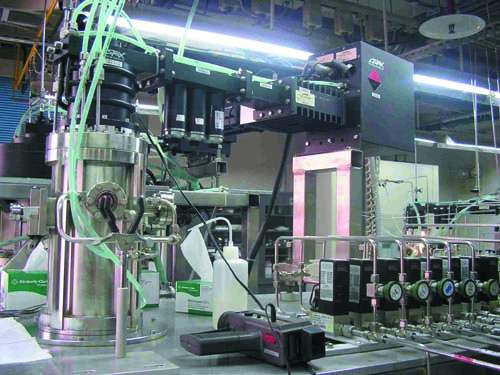
Microwave
Plasma Enhanced Chemical Vapor Deposition (MWCVD)
.
Microwave
Plasma Enhanced Chemical Vapor Deposition (MWCVD)
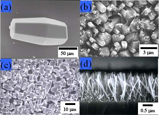
Different structure of silicon carbon nitride : (a) single crystal, (b) polycrystalline film, (c) oriented film and (d) nanorods.
Crystalline silicon carbon nitride : A wide band gap (3.8-4.7eV) semiconductor.
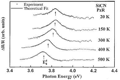
The experimental piezoreflectance (PzR) spectra (dotted curves) of SiCN at 20, 150, 300, 400, and 500 K, respectively. The solid curves are least-squares fits to the first derivative of a Lorentzian profile, which yields the direct band-to-band transition energy indicated by the arrow.
L. C. Chen, C. K. Chen, S. L. Wei, D. M. Bhusari, K. H. Chen, Y. F. Chen, Y. C. Jong, Y. S. Huang, Appl. Phys. Lett., Vol. 72, No. 19 (1998).
Crystalline SiCN : a hard material (30 GPa) rivals to cubic BN.
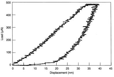
A typical indentation response of SiCN crystal deposited by microwave CVD at 1000oC.
L.C. Chen, a, K.H. Chen, S.L. Wei, P.D. Kichambare, J.J. Wu, T.R. Lu, C.T. Kuo, Thin Solid Films 355-356, 112 (1999).
Excellent field emission property of quasi-aligned SiCN nanorods
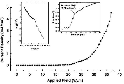
Field emission J –E curve and the corresponding F–N plot of the SiCN nanorods.
F. G. Tarntair, C. Y. Wen, L. C. Chen, J. J. Wu, K. H. Chen, P. F. Kuo, S. W. Chang, Y. F. Chen, W. K. Hong, H. C. Cheng, Appl. Phys. Lett. 76, 2630 (2000).
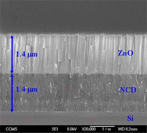
Application of nanocrystalline diamond (NCD) : surface acoustic wave (SAW) device
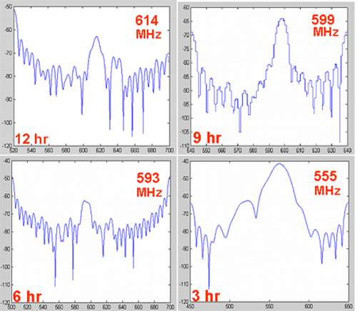
Characteristics of 0th SAW (surface acoustic wave) spectra
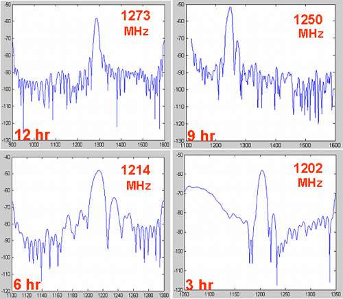
Characteristics of 1st SAW (surface acoustic wave) spectra
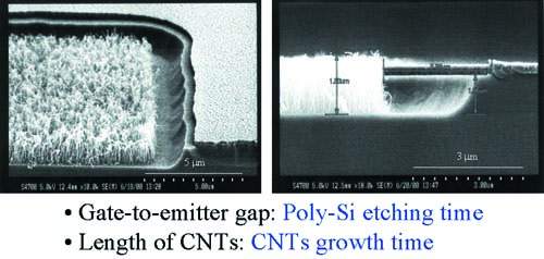
Gated CNT-FED with controllable parameters
Gated CNT-FED, anode I-gate V characteristics
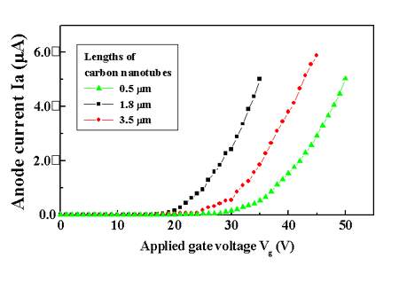
Gated CNT-FED with slightly over-gate exhibits optimized FE performance.
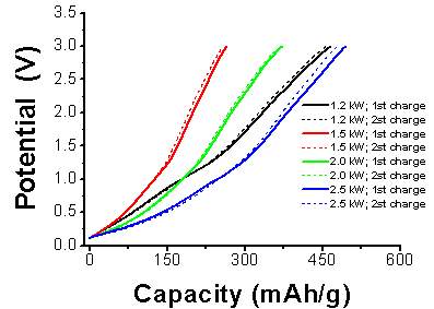
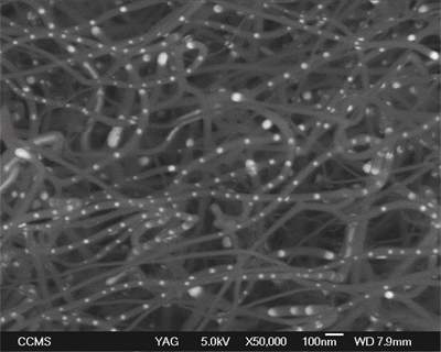
Discharging capacity behavior of CNTs grown under different microwave power
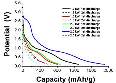
Charging capacity behavior of CNTs grown under different microwave power
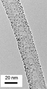
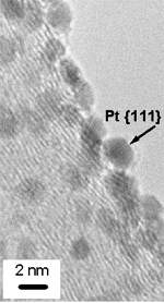
Narrow size distribution of Pt nanoparticles on carbon nanotubes
![]()
![]() .
Electron Cyclotron Resonance
Plasma Enhanced Chemical Vapor Deposition
(ECRCVD)
.
Electron Cyclotron Resonance
Plasma Enhanced Chemical Vapor Deposition
(ECRCVD)
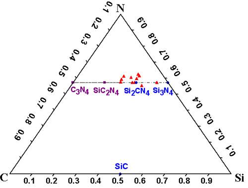
The tie-line between Si3N4 and C3N4 established in the samples produced by the ECRCVD
‘Progress and Status of SiCN: a New Wide Band Gap Material’, L. C. Chen, K. H. Chen, J.-J. Wu, D. M. Bhusari and M. C. Lin, Chapter 2, pp. 73-125, in H. S. Nalwa, Ed., Si-Based Materials and Devices, Academic Press, 2001.
Generally applicable self-masked dry etching technique for nanotip array fabrication
|
|
|
|
|
|
|
|
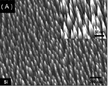
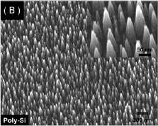
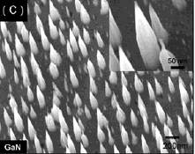
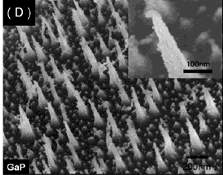
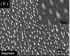
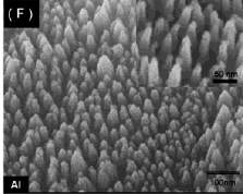
Tilted top-view FESEM morphologies of the nanotip arrays fabricated by the self-masked process of various substrates: (A) single-crystal silicon (Si); (B) polycrystalline silicon (poly-Si); (C) epitaxial gallium nitride (GaN) film on sapphire; (D) single-crystal gallium phosphide (GaP); (E) sapphire; and (F) aluminum. The insets show their corresponding magnified images.
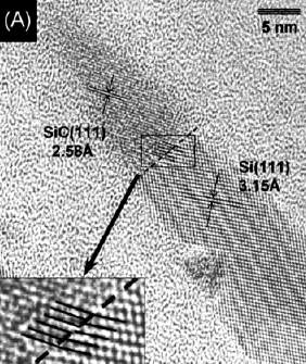
HRTEM image of the Si nanotip revealing a SiC cap formed on top of the tip. Inset shows the magnified HRTEM image of the interface between Si and SiC cap on which the lattice mismatch of Si/SiC = 4:5 can be observed.
C. H. Hsu, H. C. Lo, C. F. Chen, C. T. Wu, J. S. Hwang, D. Das, Jeff Tsai, L. C. Chen, K. H. Chen, Nano Lett. 4, 471, 2004.
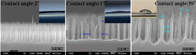
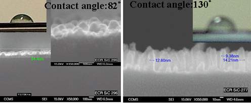
Super hydrophilic to hydrophobic, sample : Si nanotips
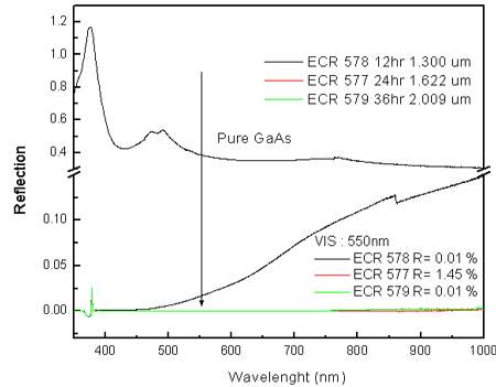
Excellent antireflection of GaAs nanotip arrays
![]()
 .
Microwave Enhanced
Metal Organic Chemical
Vapor Deposition (MWMOCVD)
.
Microwave Enhanced
Metal Organic Chemical
Vapor Deposition (MWMOCVD)
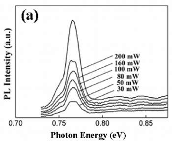
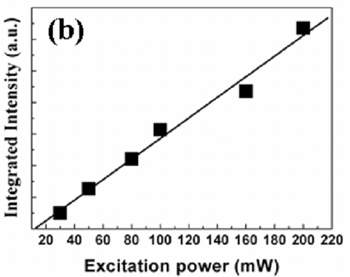
The infrared-photoluminescence (IR-PL) spectra of InN nanobelts.