PI: Prof. Chun-Wei Chen (Department of Materials Science and Engineering)
Researchers:
Prof. Chun-Wei Chen (Department of Materials Science and Engineering)
Prof. Chia-Wen Wu (Department of Chemical Engineering)
Dr. Fang-Cheng Chou (Center for Condensed Matter Sciences)
1. 2D Layered Single Crystals Growth And Design
2. 2D Atomic Layer Materials Growth And Design
The extended family of 2D materials has grown rapidly during last decade since the first isolation of graphene. Here, we would like to establish a growth platform covering mechanical exfoliation of layered single crystals, direct growth methods such as CVD, and liquid-phase exfoliation to provide unique high-quality 2D materials for the exploration of various novel physics and functionality. Prof. Chun-Wei Chen, who is one of the most recognized 2D materials research scientists in Taiwan and has received international visibility with several pioneering discoveries in this field, will be responsible for this subproject of 2D atomic layer materials.
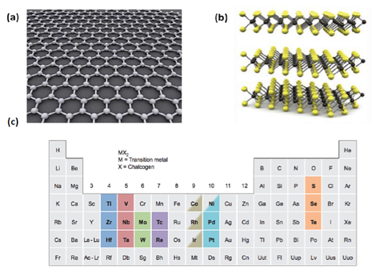
(a) 2D materials by mechanical exfoliation: The main advantage of using mechanical exfoliation to obtain 2D materials is that it may provide high-quality 2D materials without possible contamination during materials preparation. Here, we aim to design/fabricate various unique 2D materials to explore the new 2D physics and functionality jointly with the other two Thrusts. TMDCs with the formula of MX2, where M is a transition metal and X is a chalcogen, offer a broad range of electronic properties from semiconducting (e.g., M = Mo, W, Zr, Hf and Ti) to metallic or semimetallic (M = V, Nb and Ta) (Fig. 2).
Figure 2: (a) 2D atomic layer materials from graphene, (b)TMDC, (c) the periodic Table showing varieties of layered TMDC.
(b) 2D materials by chemical vapor deposition (CVD): CVD is a method that can produce relatively high quality 2D materials, potentially on a large scale in contrast to the mechanical exfoliation method. By carefully controlling the kinetic processes involved in CVD, one can obtain a desirable architecture with targeting applications. High quality TMDCs containing C–M–C structure (C = chalcogen, M = metal) will be grown by CVD techniques. One avenue of research that seems particularly promising with 2D TMDCs is electro-/photo-catalysis for the hydrogen evolution reaction and/or solar fuels, where the catalytically active sites are exposed due to the atomically thin nature of the nanosheets or defect engineering. Dr. Li-Chyong Chen, whose team is specialized in vapor depositions, will be responsible for this subproject.
Figure 3: TiO2 atomic sheets and atomic layer-by-layer deposition of 2D oxides van der Waals heterostructures based on solution processing for large-area applications.
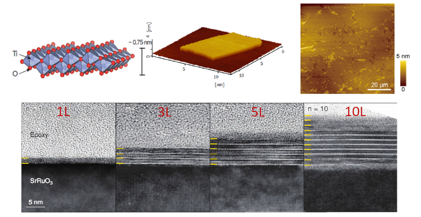
(c) 2D oxide materials by liquid phase exfoliation and assembly: Another powerful method of preparing 2D materials is based on liquid-phase exfoliation, where solution synthesis of 2D crystals by controlling the charge on individual flakes in suspensions can be obtained. We have recently developed the unique technique (jointly with NIMS, Japan) to obtain monolayer 2D TiO2 using chemical exfoliation process. These titania naonsheets, consisting of TiO6 octahedra joined together via edge-sharing to form two-dimensional lattice, have thickness approximately 1 nm and lateral dimension of 10-30 µm. By LB- film deposition process, atomic layer titania nanosheets can be easily deposited on any substrate with a well-controlled thickness (Fig. 5). Many other 2D atomic oxides can be also explored through this unique technique such as MnO2, MoO3, RuO2, perovskite oxides etc.
3. Atomic Archiecture
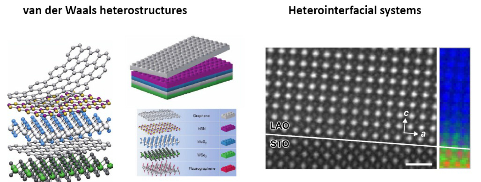
Atomic architectures consisting of 2D materials may exhibit novel properties by atomic or molecular designs and functionalities. These atomic architectures can be formed either by direct growth or by engineering stacking methods. For instance, 2D atomic heterostructures consisting of individual layers held together by vdW forces without surface dangling bonds exhibit intriguing physical properties different from those of the conventional thin film heterostructures with covalent bonding between atoms at the hetero-interface. Here, three types of 2D atomic architectures: (a) 2D vdW heterostrcutures, (b) heterointerfacial systems, and (c) 2D metal-organic frameworks (MOF) will be developed.
Figure 4: 2D vdW heterostrcutures (left), heterointerfacial systems (right).
(a) van der Waals heterostructures: Emergent 2D materials exhibit various metallic, semiconducting and insulating properties and offer an unprecedented flexibility in the creation of the so-called van der Waals heterostructures with a variety of properties, bringing a new research field of “artificial crystals” (Fig. 6(left)). In an artificial crystal, each layer acts simultaneously as the bulk material and the interface, thus reducing the amount of charge displacement within each layer. We plan to develop various vdW heterostructures by assembling the vast variety of the 2D materials available in our team. It would provide a unique platform to explore the device operation and novel functionality at the atomic level.
(b) Heterointerfacial systems: The geometrical simplicity of coherent interfaces provides an optimal platform for tackling the pristine effect of strains on 2D interfacial charges in oxide heterostructures. It has been demonstrated that the coherent biaxial compressive/tensile strains can tailor the metallic 2D electron gas at the LaAlO3/SrTiO3(STO) interface and switch the 2D interfacial conductivity of the RTiO3/STO heterostructures (R, rare-earth elements). A good example is the observation of 2D interfacial-charge condensation into 1D electron chains by the misfit-dislocation strain field across the NSMO/STO interface [Nature Communication 5, 3522 (2014)]. More extensive investigation of such novel atomic-scale heterointerfacial systems will be performed in Thrust II.
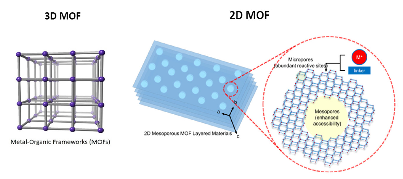
Figure 5: Self-assembly of metal ions and organic linkers for synthesis of 2D MOFs (right)
(c) 2D atomic layered nanoporous metal-organic frameworks (2D MOFs): MOFs are a crystalline porous material composed of metal nodes and organic linkers, where the physicochemical properties of MOFs can be controlled through careful selection of the inorganic or organic precursors. Particularly, the chemical sensing and biosensing, as well as energy storage applications of MOF (Fig.7) have been intensively studied. 2D MOF materials with designed structures have the unique advantages to increase the ion-accessible surface area and to improve the ion transport efficiency and become the potential functional materials. Prof. Chia-Wen Kevin Wu will be responsible for this subproject, who has been the pioneer researcher in this field of nanoporous materials and has just published an invited review article entitled “Strategies for improving the functionality of zeolitic imidazolate frameworks: Tailoring nanoarchitectures for functional applications” [Advanced Materials 29, 1700213 (2017)].