凝態中心朱明文博士主持
研究成員:
朱明文博士(臺大凝態中心)
白偉武博士(臺大凝態中心)
張玉明博士(臺大凝態中心)
溫政彥教授(臺大材料系)
邱雅萍教授(臺大物理系)
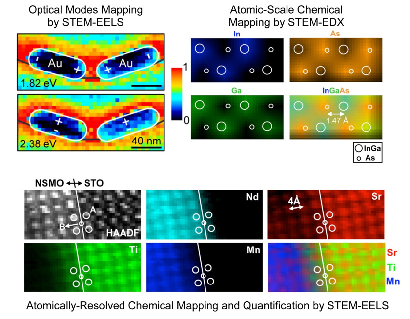
1. Atomic-Scale Electron Spectroscopy:
2. Probing 2D Materials in Green Energy by In-Situ TEM/STEM
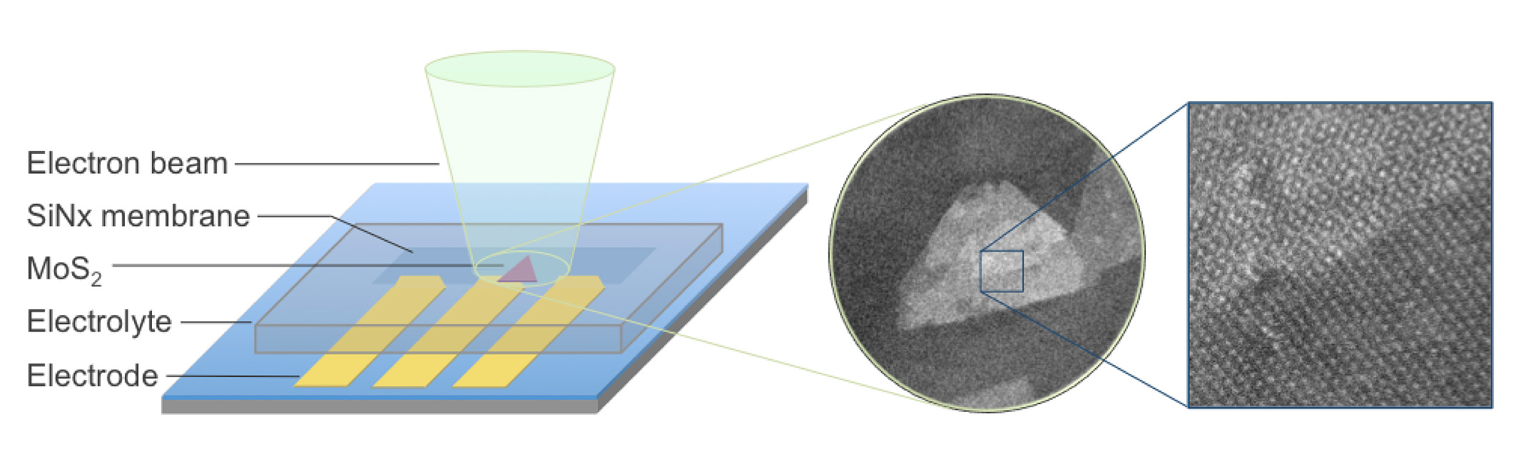
Recent progress in transmission electron microscopy (TEM) allows researchers to perform in-situ observations inside microscopes for reactions in liquid or those under the ambient gas pressure. Such an approach opens up opportunities for us to study the dynamics of electrochemical reactions and simultaneously obtain the physical information relating to the microstructures with sufficient spatial resolution. We are focusing on probing the active sites on solid phase catalytic materials by in-situ TEM, in particular 2D transition metal dichalcogenide, e.g. MoS2. Identifying the active sites and understanding the underlying mechanisms are essential for designing suitable and economic catalytic materials for electrocatalyic or photocatalytic hydrogen evolution reactions (HER).
3. XSTM Probing of Oxide Interfaces, Domain Walls, and 2D Materials
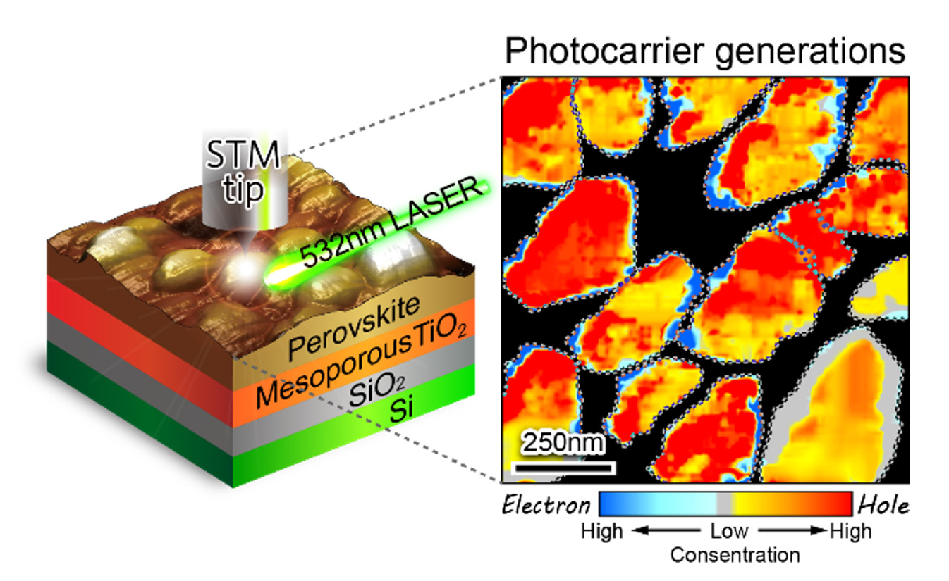
Cross-sectional Scanning Tunneling Microscopy/Spectroscopy (Dr. Ya-Ping Chiu):: Motivated by the emerging phenomena occurred at interfaces, to elucidate the fundamental mechanisms that pertain in these heterostructures is the objective in my lab. We employ cross-sectional scanning tunneling microscope (XSTM) with samples cleaved in situ in an ultrahigh vacuum chamber to study a delicate interplay of different correlated physical effects and relate these to the electronic, ferroelectric, and magnetic interface properties at the interfaces. Meanwhile, the XSTM measurements combined with light illumination provide the opportunity to study the physics at interfaces, which are crucial for improving the efficiencies of charge generation, transport, and collection of solar cells.
4. Emergent Electronic Instability and Topological States of Low-Dimensional Materials
Low-dimensional materials tend to have a stronger propensity to electron correlation and electronic instability. These can lead to various ground states such as superconductivity, charge density waves, and ordered magnetism. Furthermore, there are two-dimensional topological phases which are potentially applicable. These ground states and their low-energy excitations and interplay can be probed by scanning probe microscopy and spectroscopy (STM/STS) at various temperature with a very high spatial (2pm vertical and 100pm lateral) and energy (< meV) resolution. The surface specificity and high resolution of STM/STS offer complementary advantages to TEM/STEM. Furthermore, the role of defects, which are important for the properties of 1D/2D materials but often neglected, can be probed by STM/STS in details. We focus on the studies of the aforementioned properties in 1D and 2D transitional metal di- and tri-chalcogenides, with possible extension to other layered materials.
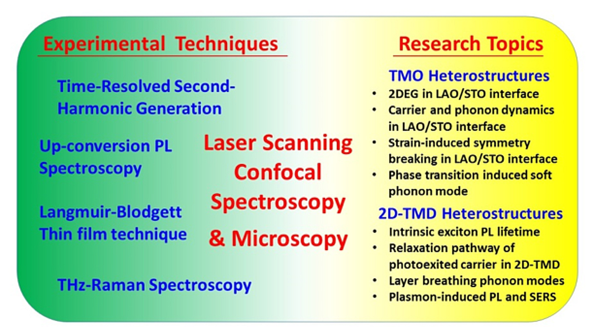
5. Ultrafast Optical Spectrosopy
To explore novel physical properties of emerging materials, we propose to construct an optical platform, so-called Ultrafast Laser Scanning Confocal Spectroscopy and Microscopy, in which we will integrate our laboratory’s core-technologies, such as femtosecond pump-probe technique, laser scanning confocal microscope, linear and nonlinear laser spectroscopic techniques developed in last two decades. This optical platform will be designed to perform temporal, spectral, and spatial mapping of emerging materials with femtosecond temporal resolution and sub-micrometer spatial resolution. The schematic diagram shown below illustrates the capabilities of this optical platform and the scientific topics and issues to be explored in next five years.